
Up-coming seminars
第25回 金沢物性セミナー
タイトル:Koopmans 準拠第一原理計算によるスモールポーラロン形成
講演者 : 裵星旻 (ベソンミン) 東北大学
日時:2026年3月5日(木)、16:00-
場所:自然科学5号館、302B室
Abstract
本講演では、一般化 Koopmans 条件を満たす第一原理計算手法に基づき、キャリア占有数に対するエネルギーの区分的線形性を回復することにより、電子および正孔ポーラロンの局在状態を体系的に解析した結果を報告する。対象として、代表的な二次元遷移金属カルコゲナイドおよび酸化チタンを取り上げ、Koopmans 準拠条件の導入がポーラロン形成の安定性および局在性の記述に本質的であることを示す。
さらに、本手法により自己相互作用誤差が効果的に低減され、低次元半導体および遷移金属酸化物におけるキャリア自己捕獲現象を信頼性高く記述できることを示す。本講演では、欠陥形成エネルギー、ドーピング特性、ならびにキャリア輸送特性の定量評価に対する本手法の有効性を示し、機能性電子材料およびエネルギー材料の理論設計への応用可能性について議論する。
Contact: 小幡正雄,obata@cphys.s.kanazawa-u.ac.jp
Past seminars
第24回 金沢物性セミナー
タイトル:Van der Waals 反強磁性体 R Te3 の磁性と密度波
日時:2026年1月14日(水)、16:30-
場所:自然科学5号館、物理会議室(404/405号室)
Abstract
References:
[1] Y. Fujisawa et al., arXiv 2507. 00750 (2025).
Contact: Yasuo Yoshida,yyoshida@se..kanazawa-u.ac.jp
参加者数: オンサイト 16名、ZOOMオンライン 12名


第23回 金沢物性セミナー
タイトル:Crystallization of heavy fermions via epitaxial strain in
spinel LiV2O4 thin film
日時:2025年12月25日(木)、17:00-
場所:自然科学5号館、物理会議室(404/405号室)
Abstract
References
[1] S. Kondo et al., Phys. Rev. Lett. 78, 3729 (1997).
[2] C. Urano et al., Phys. Rev. Lett. 85, 1052 (2000).
[3] K. Takeda et al., Physica B 359, 1312 (2005).
[4] U. Niemann, Y.-M. Wu, R. Oka et al., Proc. Natl. Acad. Sci. USA 120, e2215722120 (2023).
[5] R. Oka et al., in preparation
Contact: Yasuo Yoshida,yyoshida@se..kanazawa-u.ac.jp
参加者数: オンサイト 12名、ZOOMオンライン 6名


第22回 金沢物性セミナー
タイトル:CeTSi(T=Co, Mn)の非自明な秩序と重い電子状態
講演者 : 谷田博司(富山県立大学)/Hiroshi Tanida (Toyama Prefecture University)
日時:2025年12月5日(金)、16:30-
場所:自然科学5号館、物理会議室(404/405号室)
Abstract
[2] H. Tanida et al., J. Phys. Soc. Jpn., 88 054716 (2019).
[3] H. Tanida et al., J. Phys. Soc. Jpn., 92 044703 (2023).
Contact: Yasuo Yoshida,yyoshida@se..kanazawa-u.ac.jp
参加者数: オンサイト 19名、ZOOMオンライン 5名


第21回 金沢物性セミナー
タイトル:超高速走査トンネル顕微鏡発光分光法による単一分子発光測定の実現
講演者 : 木村 謙介(理研)/ Kensuke Kimura (Riken)
日時:2025年11月28日(金)、16:30-
場所:自然科学5号館、物理会議室(404/405号室)
Abstract
[3] T. L. Cocker, et al., Nat. Photon. 7, 620 (2013). [4] K. Yoshioka, et al., Nat. Photon. 10, 762 (2016). [5] K. Kimura, et al., ACS photon. 8, 982 (2021).[6] K. Kimura, et al., Science 387, 1077 (2025).
Contact: Yasuo Yoshida,yyoshida@se..kanazawa-u.ac.jp
参加者数: オンサイト 16名、ZOOMオンライン 3名


第20回 金沢物性セミナー
タイトル:Strain band engineering for anomalous transverse transport properties
講演者 : Susumu Minami(Kyoto University)
日時:2025年8月5日(金)、17:30-
場所:自然科学5号館、第7講義室・Zoom
Abstract
Strain engineering is a well-known approach to optimizing material performance in material science and engineering. For example, strained silicon technology has achieved enhanced chip performance by improving carrier mobility through controlled lattice deformation[3]. Since the intrinsic contribution of ANE originates from topological band structures and the associated Berry curvature, strain engineering could be a promising approach to enhance ANE.
In this seminar, I will present examples of applying strain engineering to optimize ANE. First-principles calculations were performed and the strain dependence of transport properties for L12-type Fe3Ga, a ferromagnetic compound, was evaluated. It was found that the enhancement of ANE and bipolarity of thermoelectric response are induced by lattice strain. Additionally, I will also present preliminary results on lattice strain effects on transport properties in collinear antiferromagnetic so-called altermagnet.
References:
[1] Y. Sakuraba, Scripta Mater. 111, 29 (2016).
[2] S. Minami, et al., Phys. Rev. B 102, 205128 (2020).
[3] R.S. Jacobse, et al., Nature 441, 119 (2006).
Contact: Fumiyuki Ishii, ishii@cphys.s.kanazawa-u.ac.jp
参加者数: オンサイト 19名、ZOOMオンライン XX名


第19回 金沢物性セミナー
タイトル:Observing dents in the atom
講演者 : Franz J. Giesssibl(Experimental and Applied Physics, University of Regensburg, 93053 Regensburg, Germany)
日時:2025年8月1日(金)、16:30-
場所:自然科学5号館、大講義室
Abstract
References
1. G. Binnig et al., Phys. Rev. Lett. 50 120 (1983).
2. G. Binnig et al., Phys. Rev. Lett. 56 930 (1986).
3. R. P. Feynman et al., The Feynman Lectures on Physics, Addison Wesley 1963.
4. F. J. Giessibl, Science 267, 68 (1995).
5. T. R. Albrecht et al., J. Appl. Phys. 69, 668 (1991).
6. S.Kitamura, M. Iwatsuki, Jpn. J. Appl. Phys. 34, L145 (1995).
7. Y. Sugawara, M.Ohta, H. Ueyama, S.Morita, Science 270, 1646 (1995).
8. F. J. Giessibl, Rev. Sci. Instrum. 90, 011101 (2019).
9. L. Gross et al., Science 325 1110 (2009).
10. M. Emmrich et al., Science 348 308 (2015).
11. F. Huber et al., Science 366 235 (2019).
12. M.F. Crommie, Science 2623 218 (1993).
13. F. Stilp et al., Science 372 1196 (2021).
14. J. Hütner et al., Science 385 1241 (2024).
Contact: 新井豊子, arai@staff.kanazawa-u.ac.jp
参加者数: オンサイト 60名、ZOOMオンライン 30名


第18回 金沢物性セミナー(日本物理学会北陸支部講演会)
タイトル:テラヘルツ光強磁場ESR装置の開発とその物性応用
講演者 : 大久保晋(神戸大学分子フォトサイエンス研究センター)
日時:2025年5月29日(木)、14:45-15:45
場所:自然科学5号館、物理会議室(404/405号室)
Abstract
物質の示す多様な相転移は電子のスピンや電荷、あるいは格子によって生まれる。測定手法の高度化、物質探索の深化によって、従来とは異なった物理的解釈がなされることは数多くみられる。我々はミクロな電子スピンを探針とする磁気共鳴である電子スピン共鳴(ESR)を強磁場下、テラヘルツ光の領域まで拡張し[1]、磁気相転移磁場を超える領域のスピン状態や整数スピン系などに応用してきた[2, 3]。さらに多周波数測定で2次元的に計測することで磁気異方性を与えるDzyaloshinsky-Moriya相互作用のDベクトルの方向を決定している[4]。また、現在は高圧力下におけるテラヘルツ光強磁場ESR測定[5, 6]やテラヘルツ光領域でも感度を失わない力検出型テラヘルツ光ESR測定法の開発[7]を通してこれまで測定が不可能だった微小試料の磁気的性質を明らかにしている。
参考文献
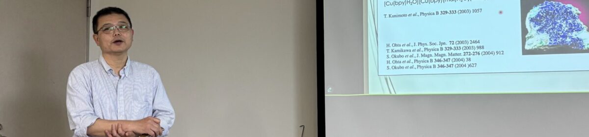
[1] SO et al., Physica B 346-247, 627 (2004).
[2] M. Yoshida, SO et al., Phys. Rev. Lett. 95, 117202 (2005).
[3] H. Ohta, SO et al., J. Phys. Soc. Jpn. 72, 2464 (2003).
[4] SO et al, J. Phys. Soc. Jpn. 86, 024703 (2017).
[5] T. Sakurai, SO et al., J. Magn. Reson. 259, 108 (2015).
[6] D. Yamamoto, SO, et al. Nat. Commun. 12, 4263 (2021)
[7] Y. Takahashi et al., Rev. Sci. Instrum. 89, 083905 (2018).
Contact: 佐藤政行, msato153@staff.kanazawa-u.ac.jp
参加者数: オンサイト 20名、ZOOMオンライン3名


第17回 金沢物性セミナー(日本物理学会北陸支部特別講演会)
タイトル:Topotronics with Magnetic Topological Materials
講演者 : Oleg Tretiakov(University of New South Wales)
日時:2025年5月13日(火)、16:30-17:30
場所:自然科学5号館、物理会議室(404/405号室)
Abstract
References:
[1] B. Göbel, I. Mertig, and O. A. Tretiakov, Phys. Rep. 895, 1 (2021).[2] B. Göbel, A. Mook, I. Mertig, and O. A. Tretiakov, Phys. Rev. B 99, 060407(R) (2019); K. Ohara, Y. Chen, J. Xia, M. Ezawa, O. A. Tretiakov, et al., Nano Lett. 22, 8559 (2022).
[3] P. A. Vorobyev, D. Kurebayashi, and O. A. Tretiakov, ArXiv:2410.10557 (2024).
[4] J. Barker and O. A. Tretiakov, Phys. Rev. Lett. 116, 147203 (2016).
[5] O. J. Amin, O. A. Tretiakov, K. W. Edmonds, and P. Wadley et al., Nature Nano. 18, 849 (2023).
Contact: 吉田靖雄, yyoshida@se.kanazawa-u.ac.jp
参加者数: オンサイト 29名、ZOOMオンライン14名


金沢物性グループ 2025年春の学会再演
日時:2025年4月10日(木)、15:00-17:00
場所:自然科学5号館、大講義室
講演者/タイトル/発表学会:
兼子裕矢/低温走査トンネル顕微鏡を用いた金表面上に蒸着した 1,10-フェナントロリンが作る構造観察/ 日本物理学会
勝田匠/磁気異方性の第一原理計算手法の開発と電界誘起変調効果への応用/東京大学物性研究所スパコン共同利用・CCMS合同研究会
岡部悠大/炎エッチングで作成したタングステン探針の調整/応用物理学会
高橋圭/電界効果によるSrVO3二重量子井戸構造の伝導制御/応用物理学会
下川 貴也/銅酸化物超伝導体Bi2Sr2CaCu2O8+δを用いた d 波超伝導探針の作製と評価/日本物理学会
石井史之/First-principles study of layer-resolved anomalous Hall conductivity in surface and interface systems・第一原理計算による薄膜・ヘテロ界面系における異常ホール効果の層分解/ APS Global Physics Summit 2025・物性研究所スパコン共同利用・CCMS合同研究会
岡林則夫/横力顕微鏡を用いた単一分子操作における摩擦の計測/ドイツ物理学会・日本物理学会
参加者数: オンサイト 40名、ZOOMオンライン1名


第16回 金沢物性セミナー
タイトル:近藤絶縁体における磁場誘起相転移
講演者 : 多田靖啓(広島大学)/ Yasuhiro Tada (Hiroshima University)
日時:2024年11月29日(金)、16:30-17:30
場所:自然科学5号館、物理会議室(404/405号室)
Abstract
本研究では、このような現状を背景に、磁場中の近藤絶縁体の基本的性質について理論的に議論する。近藤絶縁体の標準的なモデルに対して平均場近似を用いて解析を行い、ランダウ量子化とゼーマン効果、及び電子間相互作用が合わさった結果として、金属絶縁体転移点近傍の磁場領域でエキシトン絶縁体的な状態が安定化することが示される。セミナーでは、実験との比較を含めてこのエキシトン絶縁体状態に関連した磁性についても議論する。
Contact: 吉田靖雄, yyoshida@se.kanazawa-u.ac.jp
参加者数: オンサイト XX名、ZOOMオンラインXX名


第15回 金沢物性セミナー(日本物理学会北陸支部特別講演会)
タイトル:物質科学とカイラリティ
講演者 : 戸川 欣彦(大阪公立大学)/ Yoshihiko Togawa (Osaka Metropolitan University)
日時:2024年11月26日(火)、16:30-17:30
場所:自然科学5号館、物理会議室(404/405号室)
Abstract
[1-4]。その発現機構は謎であり、関心を集めている。講演ではカイラリティ誘起スピン選択性(Chirality-Induced Spin Selectivity:CISS)やカイラルフォノンなど動的な偏極現象を題材として物質中におけるカイラリティの意義を論じたい[5-7]。
参考文献:
1. A. Inui et al., PRL 124, 166602 (2020).
2. K. Shiota et al., PRL 127, 126602 (2021).
3. K. Ishito et al., Nat. Phys. 19, 35 (2023).
4. K. Ohe et al., PRL 132, 056302 (2024).
5. Y. Togawa et al., JPSJ 92, 081006 (2023).
6. 戸川欣彦ら, 数理科学 693, 9-15 (2021): 日本物理学会誌 76, 646 (2021).
7. 固体物理 2024年11月 特集号「物質科学におけるカイラリティ」.
Contact: Kei Takahashi, keitakahashi@se.kanazawa-u.ac.jp
参加者数: オンサイト 15名、ZOOMオンライン 20名


第14回 金沢物性セミナー
タイトル:Van der Waals Epitaxy of Magnetic Transition Metal Dihalides
講演者 : Amina Kimouche (University of Potsdam. Germany)
日時:2024年11月11日(月)、16:30-17:30
場所:自然科学5号館、物理会議室(404/405号室)
Abstract
There has been a growing interest in exploring two-dimensional (2D) materials beyond graphene. Starting from 2017, new platforms have been discovered with which magnetism at low dimensions is explored. The introduction of a variety of atomically thin magnetic crystals like transition metal dihalides (TMHs) has inspired efforts to not only understand the nature of magnetism but also to investigate the growth mechanism in these magnetic crystals. In this regard, nickel bromide and manganese iodide monolayer islands were grown on metallic substrates. I will show how Low Temperature Multimodal Scanning Probe Microscopy (SPM) imaging combined with Kelvin Probe Force Microscopy (KPFM) and Magnetic Force Microscopy (MFM) can reveal a ferromagnetic ground state persisting even in the monolayer regime. Occasionally, various phases have been formed giving rise to a reach variety of electronic structures as revealed by KPFM. These van der Waals materials are expected to open a wide range of possibilities for quantum applications.
Contact: Toyoko Arai, arai@staff.kanazawa-u.ac.jp
参加者数: オンサイト 18名、ZOOMオンライン 7名


第13回 金沢物性セミナー
タイトル:Critical Materials: Atom-by-Atom Investigations and Manipulations of Rare Earth Complexes for Energy and Quantum Applications
講演者 : Saw Wai Hla (Ohio University, Argonne National Laboratory)
日時:2024年10月17日(木)、16:30-17:30
場所:自然科学5号館、物理会議室(404/405号室)
Abstract
[2] T.M. Ajayi, V. Singh, K.Z. Latt, S. Sarkar, X. Cheng, S. Premarathna, N.K. Dandu, S. Wang, F. Movahedifar, S. Wieghold, N. Shirato, V. Rose, L.A. Curtiss, A.T. Ngo, E. Masson, and S.-W. Hla. Nat. Commun. 13, 6305 (2022).
[3] T.M. Ajayi, N. Shirato, T. Rojas, S. Wieghold, X. Cheng, K. Z. Latt, D. J. Trainer, N. K. Dandu, Y. Li, S. Premarathna, S. Sarkar, D. Rosenmann, Y. Liu, N. Kyritsakas, S. Wang, E. Masson, V. Rose, X. Li, A. T. Ngo, & S.-W. Hla. Nature 618, 69-73 (2023).
Contact: 吉田靖雄, yyoshida@se.kanazawa-u.ac.jp
参加者数: オンサイト 24名、ZOOMオンライン 4名


第12回 金沢物性セミナー
タイトル:熱電効果で探る2次元超伝導体の磁束状態:量子相転移と非平衡相転移
講演者 : 家永紘一郎(山口大学)/ Koichiro Ienaga (Yamaguchi University)
日時:2024年9月9日(木)、16:00-17:00
場所:自然科学5号館、物理会議室(404/405号室)
Abstract
① 2次元超伝導体はゆらぎの影響を強く受けるため,厚い超伝導体とは大きく異なる性質を示す。ゆらぎには,⾼温で顕著になる熱的なゆらぎと,極低温で重要となる量⼦的なゆらぎがあり,後者は様々な興味深い現象を引き起こすと予想されている。しかし,これまでの多くの実験は電気抵抗測定に限られていたため,完全な実証には至っていない。我々は,極低温・高磁場域で予想されている,絶対零度でも凍結しない磁束の量子液体の存在を,熱電効果測定を用いて実証した[4-6]。
② 超伝導体内の磁束は,温度や磁場の減少により液体相から固体相へと秩序化する。この秩序化は,比熱測定によって熱的(古典的)な相転移であることが示されている。一方で,外部電流で磁束への駆動力を増加させた場合には,液体状フローから格子状フローへと動的な構造の秩序化が生じることが知られている。この秩序化が駆動力をパラメータとした非平衡相転移であることを,フロー方向に垂直な電圧応答の測定[7]に加え,電流駆動中の熱電効果測定[8]により実証した。
参考文献:
[1] G. Blatter, et al., Rev. Mod. Phys., 66, 1125 (1994).
[2] C. Reichhardt and C. J. Olson Reichhardt, Rep. Prog. Phys. 80, 026501 (2017).
[3] 大熊哲, 固体物理 51, 547 (2016).
[4] K. Ienaga, et al., Phys. Rev. Lett. 125, 257001 (2020).
[5] 家永紘一郎, 大熊哲, 固体物理 55, 723 (2020).
[6] K. Ienaga, et al., Nature Commun. 15, 2388 (2024).
[7] S. Maegochi, K. Ienaga, and S. Okuma, Sci. Rep. 14, 1232 (2024).
[8] 家永紘一郎 他, 日本物理学会2024年 春季大会 19aF1-4.
Contact: 吉田靖雄, yyoshida@se.kanazawa-u.ac.jp
参加者数: オンサイト 12名、ZOOMオンライン 7名


第11回 金沢物性セミナー(日本物理学会北陸支部特別講演会)
タイトル:一つの分子を原子の大きさだけ動かす際の摩擦
講演者 : 岡林則夫(金沢大学)/ Norio Okabayashi (Kanazawa University)
日時:2024年6月11日(火)、16:30-17:30
場所:自然科学5号館、物理会議室(404/405号室)
Abstract
この問題を解決するために、銅の単結晶表面に吸着した一酸化炭素分子とプローブ顕微鏡の金属探針先端との相互作用に着目した研究を推進し[3-5]、更に、探針による一酸化炭素分子の操作およびその際の静止摩擦・動摩擦の解明へと研究を展開してきた[6,7]。具体的には、原子間力顕微鏡を用い分子におよぼされる力場ならびに分子の構造変化におけるエネルギー散逸を測定し、走査型トンネル顕微鏡による振動分光により探針下の分子の振動状態・吸着状態を調べ、第一原理計算を用い現象の解釈を行った。そして、(1)探針を分子に近づけることで生じる引力や斥力に対応して、分子の振り子運動に対応する振動モードのエネルギーが変化すること、(2)斥力が強くなると分子にとって安定なサイトが、銅原子の直上(トップサイト)から、銅原子と銅原子の間(ブリッジサイト)に変わること、(3)探針を表面に近づけ遠ざけることを繰り返すと、分子がトップサイトとブリッジサイトの間を行き来し、その際にエネルギー散逸が発生すること、を見出した。更に、このようなブリッジサイトにおける一酸化炭素分子の吸着が、探針からの力による分子操作とその際に生じる動摩擦を理解するうえで重要であることを見出した。講演会では、これらの研究成果について説明するとともに、今後の研究展望を述べる。
参考文献
[1] D. M. Eigler and E. K. Schweizer, Nature 344 (1990) 524.
[2] M. Ternes, C. P. Lutz, C. F. Hirjibehedin, F. J. Giessibl, A. J. Heinrich. Science 319 (2008) 1066.
[3] N. Okabayashi, A. Gustafsson, A. Peronio, M. Paulsson, T. Arai, and F. J. Giessibl, Phys. Rev. B 93 (2016) 165415
[4] N. Okabayashi, A. Peronio, M. Paulsson, T. Arai, and F. J. Giessibl, PNAS 115 (2018) 4571
[5] 岡林則夫、日本物理学会誌 75 (2020) 279
[6] N. Okabayashi, T. Frederiksen, A. Liebig, F. J. Giessibl, Phys. Rev. Lett. 131 (2023) 148001
[7] N. Okabayashi, T. Frederiksen, A. Liebig, F. J. Giessibl, Phys. Rev. B 108 (2023) 165401
Contact: 吉田靖雄, yyoshida@se.kanazawa-u.ac.jp
参加者数: オンサイト 18名、ZOOMオンライン 28名


*3月15日(金)に金沢大学駅前サテライトにおいて金沢物性科学研究会が行われました。
第10回 金沢物性セミナー
タイトル:点接合分光法を用いた近藤格子物質の電子状態測定
講演者 : 志賀雅亘(九州大学)/ Masanobu Shiga (Kyushu Univ.)
日時:2024年3月14日(木)、16:30-17:30
場所:自然科学5号館、物理会議室(404/405号室)
Abstract
本セミナーでは、はじめに、近藤格子物質で発現する重い電子状態などの量子現象について概説する。その後、近藤格子物質の電子状態についての理論・実験研究について紹介する。最後に、我々が行った近藤格子物質のPCS実験[4-7]について説明する予定である。 [1] A. C. Hewson, The Kondo Problem to Heavy Fermions (Cambridge University Press, Cambridge, 1993).
[2] S. Ernst, et al., Nature (London) 474, 362 (2011).
[3] W. K. Park, et al., Phys. Rev. Lett. 108, 246403 (2012).
[4] M. Shiga, et al., Phys. Rev. B 100, 245117 (2019).
[5] M. Shiga, et al., Phys. Rev. B 103, L041113 (2021).
[6] M. Shiga, et al., Phys. Rev. B 108, 195130 (2023).
[7] T. Takahashi, M. Shiga, et al., J. Phys. Soc. Jpn. 93, 023704, (2024).
Contact: 吉田靖雄, yyoshida@se.kanazawa-u.ac.jp
参加者数: オンサイト 20名、ZOOMオンライン 6名


第9回 金沢物性セミナー
Title: Large-Scale DFT Study of Heterostructure 2D Materials
Speaker: Muhammad Y. H. Widianto (Dept. Mathematics ITS and MANA-NIMS)
Date: 27th February 2024, Tuesday, 9:00-10:30
Place: Lecture room 6 in the 5th building
Abstract
References:
1. K. Uchida, S. Furuya, J-I. Iwata, A. Oshiyama, PRB 90, 155451 (2014).
2. F. Haddadi, QS. Wu, A. J. Kruchkov, O. V. Yazyev, Nano Lett., 20, 2410-2415 (2020).
3. M. Long et. al, npj Com. Mat., 8, 73 (2022).
Contact: Fumiyuki Ishii, ishii@cphys.s.kanazawa-u.ac.jp
第8回 金沢物性セミナー
Title:Atom-by-atom electron spin resonance: towards qubit platforms at the atomic scale
Speaker : Soo-hyon Phark (Center for Quantum Nanoscience, Institute for Basic Science & Ewha Womans University)
Date:11th of December (Mon), 2023, 10:30-11:30
Place:Large lecture hall in the 5th building
Abstract
References:
1. D. M. Eigler, E. K. Schweizer, Nature 344, 524–526 (1990).
2. S. Baumann et al. Science 350, 417-420 (2015).
3. K. Yang et al. Science 366, 509-512 (2019).
4. Y. Wang et al. npj Quantum Info. 9, 48 (2023).
5. S. Phark et al. Adv. Sci. 10, 2302033 (2023).
6. S. Phark et al. ACS Nano 17, 14144 (2023).
7. Y. Wang et al. Science 382, 87-92 (2023).
Contact: Yasuo Yoshida, yyoshida@se.kanazawa-u.ac.jp
The number of participants, onsite: 13, Zoom online:18


第7回 金沢物性セミナー
タイトル:超伝導化した準結晶における自発的磁束ピン留め
講演者 : 永井佑紀(原子力研究機構)/ Yuki Nagai (JAEA)
日時:2023年12月5日(火)、16:30-17:30
場所:自然科学5号館、物理会議室(404/405号室)
Abstract
そこで、我々は、このような非一様性を検出できる方法を提案するため、超伝導磁束に着目した。超伝導磁束の位置は自由エネルギー極小となる位置に配置されるため、超伝導秩序変数の空間的非一様性を超伝導磁束の振る舞いによって検出できるのではないかと考えた。
本講演では、シミュレーションによって、超伝導磁束が秩序変数の空間的非一様性によって自発的にピン留めされることを示す[2]。 [1] K. Kamiya et al., Nat. Commun. 9, 154 (2018).
[2] YN, Phys. Rev. B 106, 064506 (2022)
Contact: 吉田靖雄, yyoshida@se.kanazawa-u.ac.jp
参加者数: オンサイト 23名、ZOOMオンライン 3名


第6回 金沢物性セミナー
タイトル:トロイダル秩序にまつわる新しい交差相関応答
講演者 : 楠瀬博明(明治大学理工学部)/ Hiroyuki Kusunose (Meiji Univ.)
日時:2023年11月21日(火)、16:30-17:30
場所:自然科学5号館講義棟2階8講
Abstract
本セミナーでは、トロイダル秩序に関する話題として、時間・空間反転対称性は破らず
鏡映対称性のみを破るフェロアキシャル秩序[1]と時間反転だけを破るフェロトロイダル
モノポール秩序[2]について紹介する。前者においては、軸性の秩序変数がベクトル量を回転させる役割を担うことから、特に電場方向に平行なスピン流を生成できる可能性があり、新しい量子伝導現象を生み出す起源になる得る。一方、後者は時間反転のみを破る秩序変数により、物理量の時間反転の性質だけを反転させる応答を生み出すことができる。これにより、電場による反強磁性の制御や電場・磁場の複合場によるカイラリティ制御などを実現できる可能性がある。これらの新しい交差相関応答について紹介したい。 [1] S. Hayami, R. Oiwa, H. Kusunose, J. Phys. Soc. Jpn. 91, 113702 (2022)
[2] S. Hayami, H. Kusunose, Phys. Rev. B 108, L140409 (2023)
Contact: 小幡正雄, obata@cphys.s.kanazawa-u.ac.jp
参加者数: オンサイト 20名


第5回 金沢物性セミナー(日本物理学会北陸支部特別講演会)
タイトル:原子層結晶における新奇スピン偏極電子/Peculiar spin-polarized electrons in atomic layer crystals
講演者 : 坂本一之(大阪大学)/Kazuyuki Sakamoto (Osaka University)
日時:2023年11月14日(火)、16:30-17:30
場所:自然科学5号館、物理会議室(404/405号室)
Abstract
参考文献:
[1] Y.A. Bychkov and E.J. Rashba, JETP Lett. 39, 78 (1984).
[2] K. Sakamoto et al., Phys. Rev. Lett. 102, 096805 (2009), Phys. Rev. Lett. 103, 156801 (2009), Nat. Commun. 4, 2073 (2013).
[3] E. Annese et al., Phys. Rev. Lett. 117, 016803 (2016).
[4] K. Kobayashi et al., Phys. Rev. Lett. 125, 176401 (2020).
[5] K. Kobayashi et al., Nano Lett. 23, 7675 (2023).
[6] S. Yoshizawa et al., Nano Lett. 17, 2287 (2017).
[7] S. Inagaki et al., Phys. Rev. Mater. 7, 024805 (2023).
世話人:吉田靖雄, yyoshida@se.kanazawa-u.ac.jp
参加者数: オンサイト 17名、ZOOMオンライン 8名


第4回 金沢物性セミナー/The 4th Condensed Matter Seminar in Kanazawa
Title: Nonlinear optics on surface and interface: nano-structure and composition analysis
Speaker: Kuang Yao Lo (National Cheng Kung University)
Date: 23rd October 2023, Monday, 16:30-17:30
Place: Lecture room #404/405 in the 5th building
Abstract
Non-destructive examination of dopant concentration is essential in advanced semiconductor fabrication. One of the main issues to be tackled by the silicon device industry for miniaturization is the production of ultra-shallow doped layers, currently a key process in the silicon technology. The symmetry of the second optical susceptibility that governs the process of RSHG is directly related to the lattice symmetry and dopant situation. Therefore, RSHG has proven to be an efficient and powerful non-destructive tool for investigating the structural and electronic properties of material implanted on the surface layer, which reveal the change of dipole structure due to varied dopant concentration in RA-RSHG spectrum. However, RA-RSHG method to inspect symmetrical dipole contribution is not suitable for doped Si thin film (DSTF) since DSTF is grown by CVD method with in-situ doping and has less crystalline property. To tackle this issue, we suggest a revised time-dependent second harmonic generation (TD-SHG) for quantifying the phosphorus (P) concentration in DSTF. The correlation between the development of electric field-induced second harmonic generation (EFISHG) and dopant concentration forms the foundation of this approach. The technique is based on analyzing the evolution of the internal photoemission induced charge trapping and the concomitant electric field induced SHG. We further demonstrate a strategy to estimate the dopant concentration by considering the Fermi-Dirac distribution and the tunneling probability, without involving the crystallinity of DSUTF. The dopant concentration between 1017 to 1020 (atom/cm3) is unambiguously evaluated by this method. The unprecedented approach of using in-situ method to reveal dopant concentration of DSUTF via time-dependent SHG constitutes an important step towards in-line monitoring and optimizing the fabrication conditions.
Contact: Yasuo Yoshida, yyoshida@se.kanazawa-u.ac.jp
The number of participants: 10


第3回 金沢物性セミナー
タイトル:鉄系超伝導:発見とその後の展開 / Iron-based Superconductors: Discovery and Subsequent Developments
講演者 : 細野秀雄(東工大)/Hideo Hosono (Tokyo Institute of Technology)
日時:2023年10月23日(月) 10:30-11:30
場所:金沢大学自然科学5号館2階大講義室
Abstract
参考文献:
H. Hosono, A. Yamamoto, H. Hiramatsu, Y. Ma,
Recent advances in iron-based superconductors superconductors toward applications,
Materials today, 21, 278-302 (2008).
世話人:小畑由紀子, yobata@se.kanazawa-u.ac.jp
参加者数: オンサイト45名、ZOOMオンライン 24名


第2回金沢物性セミナー/The 2nd Condensed Matter Seminar in Kanazawa
Title: Effects of electron wave function in optoelectronics and transport
Speaker: Eddwi Hesky Hasdeo [Badan Riset dan Inovasi Nasional (BRIN), Indonesia & Université du Luxembourg]
Date: 1st September 2023, Friday, 15:00-16:00
Place: Lecture room 5 in the 5th building
Abstract
a non-trivial way. The chief example is the Berry curvature that
leads to anomalous electron velocity. In this talk, we will explore
several phenomena of such effects in optoelectronics and transport.
Firstly, spatial gap inversion induces topological boundary states in
bilayer graphene. We investigate the collective motion (plasmons) of
the topological states [1]. Next, we show non-trivial optical
responses of anomalous Hall materials such as cyclotron motion
without magnetic field and dynamical Hall currents without breaking
time reversal symmetry [2,3]. Finally, I will talk about the effect
of wave functions in electron hydrodynamics [4,5].
References
[1] EHH & JCW Song, Long-lived domain wall plasmons in gapped bilayer
graphene, Nano Letters 17, 7252 (2017).
[2] EHH, AJ Frenzel, JCW Song, Cyclotron motion without magnetic
field, New Journal of Physics 21, 083026 (2019).
[3]JM Adhidewata, RWM Komalig, MS Ukhtary, ART Nugraha, BE Gunara,
EHH, Trigonal warping effects on optical properties of anomalous Hall
materials, Physical Review B 107, 155415 (2023).
[4]EHH, J Ekström, EG Idrisov, TL Schmidt, Electron hydrodynamics of
two-dimensional anomalous Hall materials Physical Review B 103,
125106 (2021).
[5]EG Idrisov, EHH, BN Radhakrishnan, TL Schmidt, Hydrodynamic
Navier-Stokes equations in two-dimensional systems with Rashba
spin-orbit coupling, arXiv preprint arXiv:2307.07408.
Contact: Fumiyuki Ishii, ishii@cphys.s.kanazawa-u.ac.jp
The number of participants: 25


第1回 金沢物性セミナー
タイトル:ESR-STMによる単原子スピン状態の自在制御
講演者 : 土師将裕(東大物性研)/ Masahiro Haze (ISSP, University of Tokyo)
日時:2023年6月9日(金) 15:00-16:00
場所:金沢大学自然科学5号館2階大講義室(zoomによるオンライン参加登録はこちら)
Abstract
参考文献
-
[1] Y. Wang*, MH* (*equally contributed) et al., npj Quantum Information 9, 48 (2023).
[2] S. Phark, MH et al., submitted.
Email: haze@issp.u-tokyo.ac.jp
世話人:吉田靖雄
参加者数: オンサイト 17名、ZOOMオンライン 28名


Information
趣旨 / Concept
2023年5月に金沢大学の数名の物性研究者により本セミナーシリーズは開始されました。このセミナーシリーズを通して、第一線で活躍する国内外の研究者から学内の若手研究者までが最新の研究内容を議論し合い、その中から共同研究や様々な人的交流が生まれることを期待します。セミナーの内容にご興味のある方は、どなたでもご参加下さい。また、セミナー幹事として関わって下さる方も歓迎します。
This seminar series was initiated in May 2023 by several condensed matter scientists in Kanazawa University. Through this seminar series, we hope that both domestic and international researchers at the forefront and young researchers within the university will discuss the latest research topics and that collaborative research and various personal exchanges will emerge from such discussions. Anyone who is interested in the seminar is welcome to attend. We also welcome those who are involved as seminar organizers.
セミナー幹事 / Organizers
石井史之、吉田靖雄、小畑由紀子、小幡正雄、新井豊子、高橋圭 / Fumiyuki Ishii, Yasuo Yoshida, Yukiko Obata, Masao Obata, Toyoko Arai, Kei Takahashi
お問い合わせ / CONtact
吉田靖雄 ・yyoshida at se.kanazawa-u.ac.jp